
By Ro Stastny
July 31, 2024
Researchers in the Bergsman Research Group have designed a multi-chamber reactor that can run simultaneous experiments to develop new photoresists used in the rapidly advancing field of microelectronics.
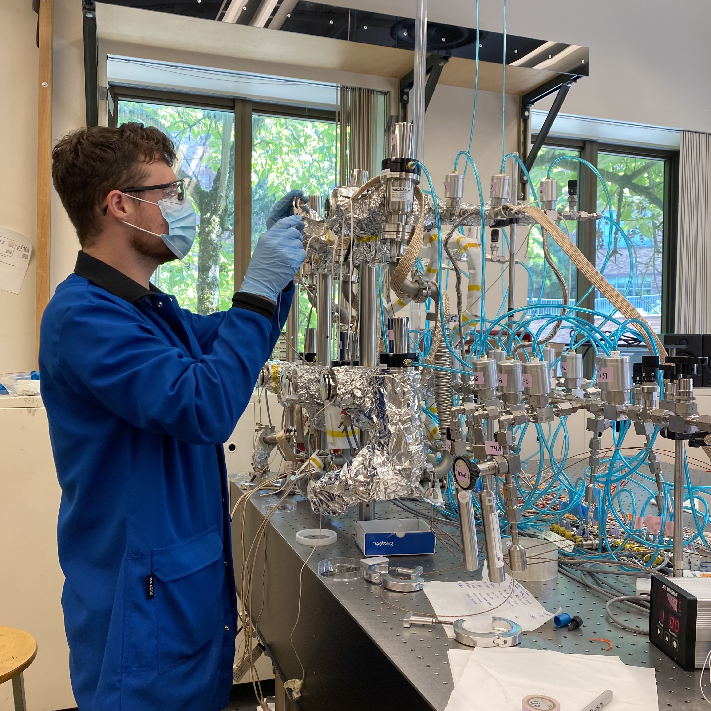
ChemE Ph.D. student Duncan Reece makes adjustments to the reactor in the Bergsman Lab.
Led by David Bergsman, assistant professor of chemical engineering, the research group aims to tackle emerging challenges in technology and sustainability using nanomaterials and interfacial engineering. Through processes like atomic layer deposition (ALD) and molecular layer deposition (MLD), researchers can develop thin films just a few atoms thick with unparalleled precision. These ultrathin films have a wide range of applications in technology, energy, sustainability, biotechnology and beyond.
Finding new photoresist materials that work well with extreme ultraviolet light (EUV) will allow for the development of smaller transistors and more powerful computers. This reactor project was funded by the Semiconductor Research Corporation, a collaboration of scientists and engineers across academic institutions, government agencies and technology companies focused on advancing critical technologies for the betterment of economic growth and national security. ChemE Ph.D. students and Bergsman Research Group members Duncan Reece and Yuri Choe outlined their process to build a new reactor made up of six independent vacuum chambers in a recent publication, which was selected for the 2024 JVST A Best ALD Paper Award.
Reactor design
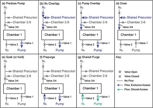
A diagram outlining the valve control system used to operate the reactor’s multiple chambers.
To achieve such a high level of atomic precision, reactive vapors that are pumped into a vacuum chamber to build up a material one atomic layer at a time. With a traditional reactor, it is not possible to run more than one experiment at the same time as these vapors expand to fill the entire chamber. Due to the number of possible combinations of materials and reactants to be tested, running each experiment individually would take a very long time, and using multiple independent reactors would be costly. As the demand for advanced nanotechnology rises, a more efficient and cost-effective method of experimentation is necessary to speed up the process.
The Bergsman Group's reactor is capable of using shared materials sources for ALD and MLD processes so that six different experiments can be conducted simultaneously without cross-contamination. A series of pipes and tubing connects each chamber to shared pieces of equipment and chemical sources. A computer then runs a program that controls which chamber each reactant vapor is sent to, and for how long.
Testing
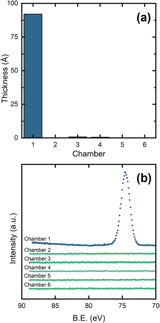
A scan of the chambers using x-ray photoelectron spectroscopy (XPS) confirms that only chamber one contains traces of the deposited materials.
Extensive testing was performed to make sure that everything was operational and that all of the valves opened and shut when prompted by the program code.
“We manually tested hundreds of joints and fittings to make sure there were absolutely no leaks,” said Reece.
A silicon wafer was placed into each chamber as the substrate for the material deposits, and then multiple alternating cycles of trimethylaluminum and water were dosed into each chamber.
To ensure that the vapors were not flowing between chambers, the researchers modified the program so that depositions were only taking place in one chamber, and then tested the composition and thickness of the substrate from each chamber again to confirm that only the specified chamber had any presence of the deposited materials, and the others did not.
When it came to the operation of the reactor, timing was a key factor down to the millisecond. Most of the valves inside the reactor are the same type, but some of the valves take just a fraction of a second longer to close. It also takes the reactant dose longer to reach chambers that are farther away from the chemical sources. To ensure no cross-contamination, the reactor had to be programmed with timing in mind, to ensure that no dosing would happen until certain valves were completely closed.
What's next
Researchers in the Bergsman Lab have immediate plans to start using this system to test reactants for semiconductor research in a new collaboration with Intel.
“So far we've run tests using aluminum and zinc. They are a bit easier to work with, but what we're trying to do now is experiment with some more challenging materials that have not been explored extensively before and are less reactive, but could work better to absorb EUV light,” said Bergsman.
Finding new photoresist materials that work well with EUV light will allow for smaller transistors, which would enable future development of more advanced microprocessors.